Welcome to “Tuesdays with Scott” segment of the Climate Change program.
Last Tuesday, I talked about the fact that much of solar cells in use are based on antiquated 70 year old technologies, which is also referred to as conventional or first generation solar cells. This is a part of a series to help educate us on how we can successfully transition away from fossil fuels. In order to do so, we need to be knowledgeable what’s currently being used and why it’s crucial that we integrate commercialization ready new technologies that can lower the cost structure of clean energy.
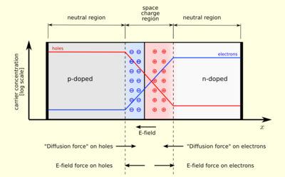
Today we talk about single junction cells or p-n junctions. We can think of them as the basic building blocks that possess the essential properties for modern electronics such as diodes, transistors, solar cells and LEDs.
Also referred to as first generation solar cells there are several types of crystalline silicon (c-Si) used in traditional wafer-based solar cells: monocrystalline silicon (mono-Si), multicrystalline silicon (multi-Si) and ribbon silicon (ribbon-Si). Multicrystalline silicon leads the global PV market with about 55 percent, followed by monocrystalline silicon at about 35 percent market share, as of 2013.
Though single junctions have efficiency about 33 percent, the conventional solar cells used in solar PV farms are of the single-junction type that have about 22 percent efficiency in reality. Single junction cells generate electricity using the single p-n junction. A p-n junction refers to the boundary between two types of semiconductor material. One type is called the p-type or the positive side that contains an excess of electron holes. A p-doped semiconductor is relatively conductive. The other is called the n-type or the negative side that contains an excess of electrons in the outer shells of the electrically neutral atoms. A n-doped semiconductor is non-conductive. By manipulating the non-conductive layer, p-n junctions allow electrical current to pass through the junction only in one direction. Bias refers to the application of a voltage across a p-n junction. A forward bias is in the direction of easy current flow and reverse bias is in the direction of little or no current flow
The p-n junction is created by doping by ion implantation, diffusion of dopants or by epitaxy. In a typical solar cell, one side of the cell is “doped” with boron, the p type, and the other side is doped with phosphorus, the n-type. In semiconductors, doped refers to introducing impurities into a pure crystal to modulate their electrical properties, and in the case of solar cells, to create a p-n junction and accompanying electric field that helps separate the electrons and electron holes formed when light is absorbed.
Solar cells made from crystalline silicon are single junction cells and these are generally more efficient than second generation solar cells based on thin-film technology.
Next week I discuss second generation thin film solar cells.
Don’t forget to subscribe to Climate Change with Scott Amyx on Amazon Alexa and give it a 5-star rating.


